

A significant development in MicroLED technology has come out of a collaboration between Lumileds and Eindhoven University of Technology. The research team has successfully demonstrated a novel approach to improving MicroLED performance by integrating metallic or dielectric metasurfaces directly into the LED structure, resulting in dramatically improved light directionality and efficiency. This development addresses two critical limitations that have hampered MicroLED development: their relatively low external quantum efficiency (EQE) and their characteristic Lambertian emission pattern, which disperses light in all directions rather than concentrating it where needed.
The research team, led by Jaime Gómez Rivas from Eindhoven University of Technology and Toni López from Lumileds, developed a novel approach that integrates nanostructured metasurfaces within the LED architecture itself. These metasurfaces consist of precisely arranged aluminum (Al) or silicon dioxide (SiO₂) nanoparticles organized in hexagonal lattice patterns. The key innovation lies in how these metasurfaces interact with the quantum wells in the LED. Rather than modifying the semiconductor material itself—which can damage the active region and reduce performance—the researchers placed the metasurface above the multiple quantum wells (MQWs) of the LED. This configuration allows the metasurface to support collective resonances that result from coupling localized resonances in nanoparticles throughout the array.
The researchers created three different types of metasurface-enhanced MicroLEDs: a hexagonal diffraction array of aluminum nanoparticles designed to achieve directional enhancement of electroluminescence; a sub-diffraction metasurface that enhances omnidirectional light outcoupling, particularly useful for smaller LED devices; and a hexagonal diffraction array using SiO₂ nanoparticles instead of aluminum to avoid Ohmic losses in the metal.
The experimental results were impressive. For the first MicroLED type, the device showed a directionality enhancement of approximately 8.6 within the emission cone of ±30°. For the third type with the SiO₂ nanoparticles, researchers achieved an integrated light extraction efficiency (LEE) of 21.4 compared to the reference device.
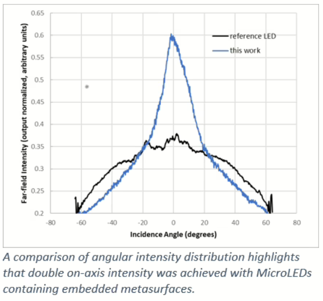
The far-field emission pattern from the first MicroLED exhibited a six-fold symmetry due to the hexagonal lattice forming the Al metasurface, enabling precise control of the emission direction. This stands in stark contrast to the reference device, which showed a standard Lambertian emission pattern without directionality.
Traditional approaches to improving MicroLED performance have significant limitations. Some methods require etching the p-doped GaN layer to enhance coupling with the metasurface, while more aggressive techniques involve etching through the active region to form nanopillar LEDs. These approaches compromise epitaxial reliability by creating defects and damaging the active region, and negatively impact internal quantum efficiency by introducing additional nonradiative recombination channels.
The newly developed approach offers several key advantages: it preserves epitaxial integrity by avoiding damage to the semiconductor layers; it offers a feasible structure for both light outcoupling enhancement and emission control; and it’s compatible with existing manufacturing technologies.
According to Lumileds, the typical Lambertian radiation pattern of LEDs creates problems for applications like augmented reality and data communication by being too wide for efficient optical coupling, while also limiting display brightness in high ambient light conditions. Their team turned to nanophotonics to address these limitations. Lumileds’ CTO emphasized that the practical advantage of their approach is the integration of metasurfaces into standard composite contact technology, which prevents semiconductor damage while using established manufacturing methods.
The technology has potential benefits across multiple applications: augmented reality displays with more efficient light coupling with optical systems, enabling smaller, lighter headsets with better battery life; high-resolution displays with enhanced luminance in bright conditions and improved energy efficiency; better directional control for optical communication systems; and potential for higher efficiency LEDs in mainstream lighting applications.
The collaboration between Lumileds and Professor Jaime Gomez Rivas’ team at TU Eindhoven continues as part of a multi-year partnership. This advancement demonstrates how narrowing the emission angle of LEDs can be achieved while also boosting efficiency—potentially just one of many beneficial results from this ongoing research effort.
What makes this research noteworthy is the specific implementation method. Most previous attempts to improve MicroLED performance involved etching the semiconductor material itself, which often damaged the active region. This approach integrates the metasurface without compromising the semiconductor structure, which is a meaningful advance.
Several research groups have been exploring metasurface approaches for LEDs over the past decade, so the fundamental concept isn’t entirely novel. However, the specific implementation and the performance improvements demonstrated (particularly the 21.4× improvement in light extraction for SiO₂ nanoparticles) represent significant progress.
Name: lily
Mobile:8613684959210
Tel:0755-27325331
Whatsapp:8618573329919
Email:sales12@huayuan-lcd.com
Add:Factory No.9, Zhongnan High-tech Intelligent Manufacturing Industrial Park, Tianyuan District, Zhuzhou,Hunan, China, 412000

